To My Readers


If this is the first time you're visiting my blog, thank you. Whether you're interested or just curious to find out about PCB reverse engineering (PCB-RE), I hope you'll find something useful here.

This blog contains many snippets of the content in my books to provide a more detailed overall sampling for my would-be readers to be better informed before making the purchase. Of course, the book contains more photos and nice illustrations, as evidence from its cover page. Hopefully, this online trailer version will whet your appetite enough to want to get a copy for yourself.

Top Review

I started doing component level repair of electronics with (and without) schematics more than 40 years ago, which activity often involves reverse-engineering of printed circuit boards. Although over the years my technical interests have shifted into particle beam instrumentation, electron microscopy, and focused ion beam technology fields, till this day——and more often than not——PCB repairs have returned multiple multi-million-dollar accelerators, FIB, and SEM instruments back to operation, delivering great satisfaction and some profit.

Many of the methods described by Keng Tiong in great details are similar to the approaches I've developed, but some of the techniques are different, and as effective and useful as efficient and practical. Systematic approach and collection of useful information presented in his books are not only invaluable for a novice approaching PCB-level reverse engineering, but also very interesting reading and hands-on reference for professionals.

Focus on reverse engineering instead of original design provides unique perspective into workings of electronics, and in my opinion books by Keng Tiong (I've got all three of them) are must-read for anybody trying to develop good understanding of electronics——together with writings by Paul Horowitz and Winfield Hill, Phil Hobbs, Jim Williams, Bob Pease, Howard Johnson and Martin Graham, Sam Goldwasser, and other world's top electronics experts.

Valery Ray
Particle Beam Systems Technologist

Tuesday, October 24, 2017

ATX Power Surprise!

Finally gotten the ATX power supply schematic redrawn and corrected all the reference designation errors:

Since it is done with Microsoft Visio, the drawing will look much better in print, better than what you see here with its limited display resolution. Can you identify the main components of the ATX power supply? The answer is also provided in the one-page scaled-down version following this two-page spanning schematic.

Now back to working on the FPT chapter...

Sunday, October 22, 2017

A Good Distraction...

While working on the FPT chapter, I got a nagging feeling that I missed out something in the power supply section of Chapter 3. As it turned out, I forgot to include the topology diagrams for the linear types and went ahead to create and include them. And since I'm at it, I thought I might as well throw in some additional stuff——an ATX power supply as a PCB-RE example.

Here's a two-page sample:


In my search for a schematic diagram that best illustrates the SMPS design aspect for an ATX model, I found one that suits my expectation in terms of layout design——except that there are a number of errors in the component designations. I decided if I want it to look good in the book, I might as well redo and clean up the drawing myself.

Will revert back to writing the FPT chapter when I'm done with this task.


Saturday, October 14, 2017

ScanCAD Edition

As mentioned in my previous post, I've come up with an interim edition for ScanCAD International Inc. while writing the chapters for the full version of the book. This special edition is now in the final works and will be delivered to ScanCAD in 1-2 weeks time. Below is a 2-page sample:


It gives a rough evaluation of the chances of doing PCB-RE using different approaches for a medium complex 4-layer board. Besides the table and charts, there's also further explanations given for the FPT, X-ray and delayering techniques (not shown). As a bonus, I have included a rare interview with the CEO of ScanCAD on his views about PCB-RE too!

Their next stop will be at Productronica 2017 in Munich, Germany on November 14-17. Interested readers in Europe who are going to this exhibition, do keep a look out for ScanCAD's booth...

Sunday, October 8, 2017

One More Chapter to Go...

I'm happy to announce that the JTAG chapter is finally completed! Here is a two-page sample of the 22 pages worth of interesting and informative work I've done.


Will take a short break and then start work with the Flying Probe Test (FPT) chapter. Hopefully, I can get the first draft of the book ready for review by end October...

Friday, September 29, 2017

Good News, Bad News

First the bad news:

My upcoming book, PCB-RE: Tools & Techniques, will be further delayed due to the non-committal attitude of the last contributor on the FPT and JTAG chapters. This is an unfortunate turn of event and I felt bad for the other contributors who have put in their time and effort, though it was not my fault entirely. In the end, I decided it is better that I write the chapters myself than to depend on someone who keeps playing the delaying game with me.

Like I put it in advance at the ending of the book:
I'm not a person who gloss over details on a subject or task I set my mind to learn or undertake, which is why contributors to the various chapters in this book can appreciate my editorial expectations on their works to ensure readers have the best overall reading experience.
And now the good news:

Bill Loving and Jeff Rupert of ScanCAD International, Inc. have been strong supporters for my book and in view of the delay, I have proposed a special ScanCAD edition to the book for their upcoming exhibitions:


They will be giving away free copies of this book and also my first engineering book The Art of PCB Reverse Engineering to existing and potential customers. So keep a lookout for ScanCAD's booth at these events:

SMTA Guadalajara 2017 - Guadalajara, Mexico - October 18-19, 2017 - USM Reps
Productronica 2017 - Munich, Germany - Nov 14-17,2017
DMC/DMSMS 2017 - Tampa FL, USA - Dec 4-7, 2017 - ScanCAD Booth 501
IPC/APEX 2018 - San Diego, CA, USA - February 27- March 01 ,2018 - ScanCAD Booth

That's all for now. Stay tune for more updates...

Sunday, September 3, 2017

Completed. Well, Not Quite...

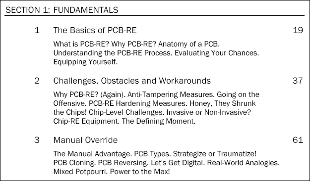
I'm happy to announced that I have completed the last chapter of Section 1 of my book, comprising three chapters on the Fundamentals of PCB-RE.


Don't be misled by the simple outline and sub-headings of these chapters. They're jam-packed with lots of interesting information and illustrations. Chapter 3 is perhaps the largest chapter of the whole book (40 pages) but overall I am rather pleased with the structures of each individual chapter, having spent much time writing and drawing the illustrations (in Visio), as well as getting the relevant photos for the topics discussed, either directly from the original sources, or requested for permission to use. All these took time and effort to liaise and collate, not to mention processing and proportioning the images so they turn out great for publishing.

My part is done, but I will be going through the completed portions while I await the two chapters for Section 2 from the last contributor, which he promised will be ready by Wednesday. Let's hope he keep to the schedule...

Friday, September 1, 2017

Image to Gerber Conversion

Early this month I mentioned an image to Gerber conversion java program that can be an alternative for those who do not want to learn or use a PCB layout program. I was informed by the programmer a few days ago that there is a new version available at Sourceforge, so I went over and downloaded the package to give it a try.


There were a few improvements made, specifically the ones I suggested, namely the ability to save the selected colors and better contrast for the WhatsThisColor dialog box when the mouse moves over a darker color background. On top of that, the ability to select which of the four color artworks to replace is a nice feature too.

If you have not give it a test drive yet, go to the following link to download the program:

https://sourceforge.net/projects/imagetogerberconverter/

It's free but if you think it's useful to you, a small donation to the programmer is a nice gesture of appreciation for sure!

Wednesday, August 30, 2017

Progress Update (Mixed Signal)

Two sample pages on reversing mixed signal PCBs which I've completed today. This time, I'm showing the portion on PCB design considerations:


The last portion will be on power supplies. I foresee that the book will hit over 320 pages when I'm done with this chapter. There's two more chapters to go, from the last contributor. Hopefully, I'll get the drafts on the Flying Probes and JTAG to incorporate into the book soon...

Friday, August 25, 2017

Progress Update (Analog PCBs)

Just completed the topic on reversing analog PCBs. Here's two sample pages:


Now going on to mixed-signal PCBs and then power supplies. Should wrap up the chapter by end of August. Then it's a final review of the various chapters before sending the draft to the Editor-in-Chief of a well-known magazine for his review.

Monday, August 21, 2017

Progress Update (Digital PCBs)

I've just completed the topic on reversing digital PCBs, and thought I'd put up two sample pages for readers to take a look:


Besides introductory notes on the various digital logic thresholds and operating voltages, emphasis on the importance of preparation work, and the steps involved in doing digital PCB-RE, I also expanded on each of the steps with illustrations and photos, followed by discussion on design considerations for this type of PCBs, peppered with informative footnotes along the way.

The way things are going for this third chapter, it's probably going to take up more pages than I had initially anticipated. Good for the readers, but certainly more work for me!

Friday, August 18, 2017

Progress Update (PCB Reversing)

In The Art of PCB Reverse Engineering I laid out detailed steps and procedures on how to recover the schematics from a physical PCB, from determining the board's accessibility, identifying components and creating a bill of materials (BOM), removing conformal coating if it is present, to gathering parts datasheet and information as a pre-requisite preparation prior to the actual work.

Systematic documentation of the process and strategic approaches for different PCB types are just as important, and I took great pains to show how this is done using Microsoft Visio as the diagramming tool of choice, first to create a layout diagram populated with component symbols that are either simple (basic geometrical entities) or smart (Visio's Smartshapes that are embedded with data and formulas), and on to producing schematics that are consistent and readable using the netlist extracted from the physical board. There are also numerous advanced topics included in that book as well.


This sequel to my first book, though aimed at giving readers a broad sweep of the industrial tools and techniques on PCB-RE,  will nevertheless still be incomplete without some mention on manual PCB-RE. My intention is to familiarize readers with the steps involved without overbearing with details, and at the same time to look at PCB-RE from a design perspective to understand important characteristics of different PCB types and in the process, gain a better chance of success.

A reader put forth this feedback to me:
Perhaps what I would like to see more in the midst of explaining component features and how to draw them in Visio is also the different characteristics and features a PCB can hold. It'll be helpful to explain why traces are drawn in a certain way, which may tell you a lot about the PCB as well as its layer design and characteristics such as grounding, shielding, vias and all the rules it must adhere to etc.
Though PCB design is not my forte, I have experimented with different PCB layout programs and know the importance of design and electrical rules checks, and had worked on quite a variety of PCBs to appreciate their underlying design considerations. Generally, the three main concerns are:

1. Electromagnetic interference (EMI)
2. Signal integrity (SI)
3. Thermal management

These factors, plus some others, ultimately affect how components are placed, the way copper layers and power planes are arranged, how signals are routed, the kind of vias to use, and whether additional heat dissipation measures are required, etc. 

And as requested by the above reader, I will first list the generic steps involved in reversing each type of PCB——digital, analog, mixed-signal, power——and then follow on with some design specifics related to each PCB type. The sequel book content will therefore compliment The Art of PCB Reverse Engineering in this respect.

Friday, August 4, 2017

Progress Update

Currently, I'm writing the final chapter in the Fundamentals (Section 1) of my book. It deals with manual PCB-RE, the advantages of doing it by hand, the types of PCBs, the need for strategies working with different types of boards, and more recently the steps involved with PCB cloning, which I've laid out in six steps. Before moving on to PCB Reversing, I mentioned one interesting Java program which I found online, while searching for raster to Gerber conversion as an alternative option for those who may not want to learn how to use a PCB layout program.

I downloaded the package from Sourceforge, installed the latest Java, setup the environment and path in the system variables, then fired up the program from the command prompt. For a test drive, I loaded a moderately complex board layout, set the color tolerance to 50, and selected the top (red), bottom (blue), silkscreen (yellow) and drill layers (brown):


The results are pretty good, though there are certain improvements that need to be made before it can be a really useful program. For those interested to see it in action, there is a YouTube video online at:

https://www.youtube.com/watch?v=RdQ_jO0g25A

I still have two chapters in waiting for Section 2, coming from an industrial engineer on FPT and JTAG. Hopefully, I don't have to wait too long for the first drafts to start integrating the contents into their respective chapters. I really hope to get the book ready for release by end August, or latest early September.

Thursday, July 13, 2017

My Upcoming Book...

The past couple of weeks I have been busy with my next book, PCB-RE: Tools & Techniques. It is a sequel to my first engineering book, The Art of PCB Reverse Engineering. Those of you who bought it will have learnt that it is a book on doing PCB-RE the manual way using Microsoft Visio as the diagramming tool of choice for properly documenting the process from start to finish.

Well, the focus of this sequel book is different. Much, much different. It is meant to give the PCB-RE practice a more complete treatment by addressing the tools and techniques used by industry experts and practitioners, and covers topics like PCB deconstruction, flying probes, ScanCAD, JTAG, clip-and-learn, Chip-off forensics and X-ray. And it will not be a one-man effort this time because I have enlisted the help of a number of highly experienced people to contribute their knowledge in the area they're good at. It will be a one-of-it's-kind book on PCB-RE. For sure!

In case you're curious, here is the front cover of the book:


For once, I get to be both the author and editor-in-charge, like John Black in his voluminous book, The System Engineer's Handbook. You will get to know the various authors in the Contribution List, the Acknowledgment, and at the end of each chapter they contributed. There are three sections to the book: Fundamentals, Tools & Techniques, Resources and an Appendix that is informative in itself.

That's all I have to say for now. If you've not gotten a copy of The Art of PCB-RE, then perhaps it's time you do, in anticipation of the sequel to it. ;)

Saturday, June 17, 2017

More PCB Layout Examples

Learning the Microsoft Visio diagramming tool is just the start of an exciting journey in creating professional quality illustrations for your engineering work. You have the option of representing the same PCB using different approaches, just like the HP power supply module example found in my book, from this:

to this with more information:


You might think that only the pros are able to produce this kind of work fit for publication. But I can assure you that if you keep at it, you will only get better with time. Skill is something that is refined through constant practice. But you've got to start somewhere. Better still, if you have someone or a book to guide you along.

Tuesday, June 13, 2017

Laying Out the PCB Artwork

If you think Microsoft Visio is only good for doing flowcharts, organizational charts, or floor plans using its supplied stencils, I hope the earlier layout drawing will change your mind set. As far as I'm concerned, Visio does a pretty amazing job with 2D technical illustrations.

I won't go into details in my blog on describing the Visio workspace, how to configure its initial settings (user and developer modes, ruler and grids, guide lines and guide points, font, text, line and fill styles, etc.), the various quick maneuvering tricks (zooming, panning, scrolling) and manipulating objects (aligning, distributing, arraying, sizing and positioning). These are all covered adequately in my book.

For simplicity's sake, I use a simple example to illustrate the steps involved in creating a PCB layout of a SCSI host adapter, as shown below:


There are four specific steps to creating the PCB layout:

1. Prepare the drawing page
2. Draw the PCB outline
3. Create the component layout symbols
4. Populate the PCB

Each of these steps are also detailed in my book so that you'll be able to replicate exactly what I've drawn, using the X-Y coordinates and the size and position properties of each object that you create, including the SCSI connector itself. As you work through the exercises, you'll come to appreciate the beauty of breaking down a seemingly complex object into basic building blocks, and then assembling them together. You will also be taught how to create sophisticated objects such as the various SMT ICs (PLCC and its socket) and their footprints in a later part of the chapter.

You'll learn the trick of creating impressive PCB layout illustrations that are professional to look at and captivate your audience in your report presentation.

Friday, June 9, 2017

Why PCB Layout Diagram?

You may be wondering why you need a PCB layout diagram for doing RE work? Well, that depends on your style of working or preference. Some might think it's a hassle and prefer to just photocopy the PCB and use it as the basis to work on the schematics. I won't stop you from doing that, but allow me to give you a word of caution from my own experience—it'll get messy and confusing as you progress, and the less than ideal resolution of most photocopy printout might prove too much for your eyes, especially if the PCB is densely populated; also, if there are missing reference designators, you'll have to manually label them. And each time you screw up and need to redo the printout, it's going to be a perpetual pain you'd wish you had a decent layout diagram to print on demand.


A PCB layout diagram serves the following purposes:

1. Proper documentation of the PCB, including missing reference designators and additional data you might care to put in, such as the BOM side by side for quick reference.

2. Ease of locating specific components since it is in electronic form and therefore searchable even across multiple pages.

3. Facilitate marking (highlighting) of probed points to allow you to view your progress and cut down on repetitive probing, saving time and reducing wear or possible damage to the PCB.

Tuesday, June 6, 2017

Why Microsoft Visio?

As the blog URL suggests, I use Microsoft Visio for all my technical illustrations. It it the tool of choice for me ever since I first used it back in 1996. The versatility of this 2D diagramming software in terms of its functions and user interface makes it easy to learn compared to other CAD or CAE programs. This has to do with its initial design concept when the original maker (Shapeware) produced and marketed it in 1992. When Microsoft acquired it in 2000, Visio was given an overhaul and integrated with Microsoft Office. Though it suffered performance issues in the earlier Microsoft releases (as usual), from the 2007 version onward the software has become better in terms of usability and programmability with an improved smartshape structural definition.

Because Visio is a general vector-based graphics editor, it is suited for a wide variety of purposes, not just limited to flowcharts, processes or organizational hierarchies. It's multiple-page feature allows flat or hierarchical representation of schematics just like most CAE tools, less the steep learning curves and rigid component representations.

Besides the PCB layout diagram which you've just seen in the previous post, below is a full-blown schematic diagram of the DS203 nano mini digital storage oscilloscope which I've redrawn from the original using, you guess it, Visio:


This drawing, along with many more illustrations, will be featured in my upcoming book PCB-RE: Tools and Techniques, the sequel to The Art of PCB Reverse Engineering. It features many experts from different fields of the PCB-RE discipline, who will share their experiences and practices on the various aspects related to this niche topic. If you have bought and enjoyed reading my first book, then it might please you to know that the best is yet to come.

So keep a look out for its release in the not too distant future.

Monday, June 5, 2017

Creating a PCB Layout (Introduction)

The first thing you need to do after the preparation work (see the aforementioned ABCDs in my previous posts), is to create a PCB layout of the board you intend to reverse engineer on. The thought of creating a PCB layout, however, may seem daunting, especially to those who do not have the experience of using a CAD program. Consider the following example from my own portfolio:


Yeah, I know what you're thinking right now. Some of you might be thinking, "Wow! Is it possible for me to draw THAT?" Others might be contemplating about giving up the idea of doing reverse engineering, "You gotta be kidding! I could never do what you did even if I try..." Hopefully there'll be some who'll respond, "I like what I'm seeing and I'm gonna give it my best shot and see what I can come up with!"

Well, it's not as complicated as the first impression you might have. The book will show you how to create these professional PCB layout diagrams using Microsoft Visio, one of the best diagramming tool out there you can find. And believe me, in the process of learning how to use this amazing piece of software, you'll be able to create virtually any kind of engineering and artistic illustration your mind can imagine. And it gets even better: Visio has a hidden gem that many casual and frequent users often missed, avoid or overlooked - Smartshapes. This too is covered in the Advanced Topics of my book, which one reader commented:

Just received my copy of your book from Amazon. Amazing! This is going to be one of the most useful books I have ever bought. Visio has always been one of my favorite tools, and I would consider myself quite an expert, but you have shown me some wonderful new tricks!

Ken Howard
Configuration Manager
Wide Area and Space Surveillance Systems Program Office
Department of Defense | Capability Acquisition and Sustainment Group

Monday, May 29, 2017

Missing Reference Designators

Sooner or later, you are going to come across PCBs with components that do not have their reference designators printed on the silkscreen layer, either due to congestion of space or by design. What then?

Well, you can do the following steps:

1. Take note of component designators that are available on the component and solder sides' silkscreen layers of the PCB. Note down the largest number for each of the group designators (e.g. R123, C99, U68, etc.).

2. Determine the arrangement or layout of the components, paying attention to the way the reference designators run on the PCB, horizontally or vertically, from left to right or vice versa. Then follow the flow by adopting either a row or column numbering pattern accordingly.

3. Make a photocopy scan of the PCB, grayscale and inverse it, and then segment it into grids as shown below. Start numbering the unmarked resistors based on the grid reference: R1A, R1B, R1C, etc.


The above example uses column numbering pattern due to the layout of the components which makes it suitable for this scheme. Sometimes the components' layout maybe haphazard or random, in which case you can still produce a grayscale-inverse artwork of the PCB, print it out and manually write on the hardcopy. This is the fastest way to assign designators, but is quite messy and error prone.

A better way is to wait till you complete drawing the Visio layout diagram of the PCB before assigning the designators (what this book teaches). This will save you a lot of trouble in case you miscount or miss-count the components and need to white-out or erase the errors and re-number the designators on paper.

Tuesday, May 23, 2017

Components Without Markings

As the size of components get smaller, it becomes impossible to label them intelligibly, or even to label them at all. 

Some manufacturers do provide laser markings on their chip capacitors to prevent surface degradation or induced micro-cracks; these codes are based on the EIA RS 198 standards which use 2- or 3-digit alphanumeric codes to represent capacitance values. With these codes, you can then look up their product datasheet reference to determine the values. For example, A5 = 100,000pF or 100nF, where N denotes the vendor NovaCap.


But what do you do with SMD components without markings?

While you're more likely to encounter chip capacitors with no markings than chip resistors, resolving the latter is a much simpler and straightforward affair. A normal digital multimeter can usually measure resistors in-circuit quite accurately without interference from adjacent components, unless there are parallel resistors or low impedance path across the resistor in question.

Unfortunately there's no way you can measure a capacitor in-circuit due to PCB track capacitances as well as induced lead and bond-wire capacitances of components around it. For the most part, you can get some hint from the usage of these SMD capacitors. You can find out more on this and other topics in the book The Art of PCB Reverse Engineering.

Saturday, May 13, 2017

Component Classifications (Part 5)

Integrated Circuits

Integrated circuits (IC) are by far the most diversified and interesting of all electronic components, from small- to medium-scale (SSI/MSI) integration like the TTL/CMOS chips, to the large and very large-scale (LSI/VLSI) peripherals and microprocessors, and finally to the ultra large-scale (ULSI) containing over one million transistors, and the wafer-scale integration (WSI) that uses the entire silicon wafer to fabricate a super-chip.


And if you think you've seen enough possible varieties of component packages in the earlier sections, think again! As of April 2014, the existing list of integrated circuit packages can be grouped under eight major categories:

Through-hole SIP, DIP, CERDIP, QIP, SDIP, ZIP, MDIP, PDIP
Surface mount CGA, CCGA, CQGP, LLP, LGA, MCM, Micro SMDXT
Chip carrier BCC, CLCC, LCC, LCCC, DLCC, PLCC
Pin grid array OPGA, FCPGA, PAC, PPGA, CPGA
Flat pack CFP, DFN, QFN, PQFN, TQFN, QFP, BQFP, CQFP, LQFP, PQFP, TQFP
Small outline SOIC, SOP, CSOP, MSOP, PSOP, QSOP, SSOP, TSOP, TSSOP
Chip-scale CSP, TCSP, TDSP, COB, COF, COG, Micro SMD
Ball grid array CBGA, FBGA, LBGA, PBGA, SBGA, TBGA, μBGA

The above list is by no means exhaustive, but it gives you an idea of the extent the world of integrated circuits encompassed. 


Note:

My book's Appendix C contains sample isometric illustrations of popular IC packages which might be useful in identifying these myriads of ICs you may come across on a PCB. Of course, it does help to know that ICs are mostly designated as U or (you guess it) IC on the PCB's solder mask.

Friday, May 12, 2017

Component Classifications (Part 4)

Had been pretty tied up with my next engineering book lately, as well as family commitments. Well, here's the next installment:


Transistors and MOSFETs

The transistor—from its humble beginning as a discrete entity in 1947 at AT&T's Bell Laboratory, to its present highly integrated forms numbering in the millions—is the basic building block of all modern electronic devices.


Transistors can be broadly classified into two types: bipolar and unipolar (also known as field-effect transistor, or FET). The bipolar transistor has three terminals labeled base, collector and emitter, and utilizes a small base current to control or switch a much larger current between the collector and emitter. As such, the BJT can function as an amplifier in the linear range, or as a switch under saturated condition. The FET also has three terminals labeled gate, drain and source, but uses a gate voltage to control the current between the source and drain. The FET can be further divided into junction FET (JFET) and insulated or metal-oxide semiconductor FET (MOSFET).

Like the diodes, military grade transistors are similarly prefixed with JAN, JANTX, JANTXV, or simply JX before their usual 2Nxxx commercial part numbers. Likewise, SMD transistors are marked with 2 or 3 alpha-numeric codes. For example, the Fairchild MMBT2222A is the equivalent of a 2N2222A TO-18 NPN transistor. There are also transistor array ICs used mainly for driving/sinking high current loads, such as the ULN2803A.

Wednesday, April 19, 2017

Component Classifications (Part 3)

Generally, passive devices have no functional gain or control over voltage or current, their controlling function is basically linear as in the case of a resistor. Active devices on the other hand has the ability to electrically control electron flow to manipulate and transform a signal's properties. For a circuit to be considered electronic, it must contain at least one active device.

Diodes and Zeners


A diode, by definition, is a two-terminal non-linear device that works on the p-n junction principle that exhibits forward and reverse biasing characteristics. There are many types of diodes, from the common rectifier to the varactor, the light-emitting to the photo-laser, and the step recovery to the zener, etc.

So what is the difference between a diode and a zener?

While a diode operates on the forward voltage region and may suffer catastrophic failure if subjected to voltages that exceed its reverse breakdown limit, the zener can safely operate on the reverse voltage region. In other words, while a diode conducts current in only one direction, a zener, by virtue of its heavy narrow junction doping, can conduct current in both directions with the ability to maintain a stable voltage in the reverse bias condition. This makes the zener ideal for applications such as voltage references in comparator circuits and voltage stabilizers in low-current circuits.

As you'd probably realized by now, unlike the axial-lead diodes, SMD packages can contain more than one diode per package type, such as the BAV99 example just mentioned. Things can get really tricky, however, when you work on PCBs with many of these SMD type components present, so it's good to download a copy of the SMD Codebook and keep it handy for quick reference.


Ps: While there are many editions of free SMD Codebook online, readers who buy my book will get a copy of the SMD Code Reference Book, which contains over 500 pages listing of more than 23,000 SMD type component markings.

Tuesday, April 11, 2017

Component Classifications (Part 2)

Before going into active components (semiconductors and ICs), let's take a look at one type of device
that is widely used in many digital and processor-based PCB designs—the crystal oscillator.


Crystal oscillators, whether excited by the host ICs which they are connected to, or powered by external sources, exhibit high quality factors (Q) above 10,000 and are suitable for use as resonators and in high stability tuned circuits.

In its simplest form, a crystal oscillator has a fixed frequency vibration with accuracy up to ±30ppm, but greater accuracy and stability can be further achieved in mission critical system using special variants like the voltage-controlled crystal oscillator (VCXO), temperature compensated crystal oscillator (TCXO), and the oven-controlled crystal oscillator (OCXO).

Tuesday, April 4, 2017

Component Classifications (Part 1)

Components are the basic building blocks in electronic circuits. They come in all shapes and sizes and perform different functions based on their electrical characteristics, some of which are simple and straightforward, while others are complex and cascaded in nature,

Generally, components are classified into discrete and integrated, the former being a single entity or unit, while the latter is made up of multiple discrete entities ranging from a few to over a million, depending on the manufacturing process and technology. These are further differentiated into passive and active components, the former requiring no external sources to power or operate, whereas the latter uses and manipulates energy to effect gain or change in a signal's condition.


Passive Discrete Components

Some examples of passive discrete components are shown in the photos below:


The resistor is one of the most basic element in an electrical circuit. Types of resistor include carbon composites, chip SMDs, PTC thermistors, aluminum clads, and networks. Second only to resistors, capacitors are one of the most common components you'll find on PCBs. Types of capacitor include electrolytics, micas, chip SMDs, radial-lead ceramics, and axial-lead tantalums.

Together with resistors and capacitors, inductors belong to the same passive linear circuit elements found in electrical circuits. Inductors and capacitors are two types of energy storage elements—the former deals with current while the later with voltage. Types of inductor include axial-lead, radial-lead, torroids, ferrite-cores, unshielded and shielded SMDs.

A fuse is a kind of resistor with low resistance and built to tolerate a certain amount of current, which if exceeded, will cause it to blow up and become an open. In other words, it's a protection device. Types of fuse include axial-lead, glass cartridges, radial, SMDs, resettable and blade.

Most relays are electro-mechanical in structure in which contacts make-and-break by means of a relay coil being energized or de-energized by a control voltage. For this reason, they are also called electrically operated switches. Types of relay include electro-mechanical, reeds, TO-5, SMDs, solid-state and hermetically sealed.

It is important to be able to identify these discrete components when doing PCB reverse engineering, especially with modern surface-mounted boards where such components are shrinking in size and their markings on the PCB are kept to a minimum.