To My Readers


If this is the first time you're visiting my blog, thank you. Whether you're interested or just curious to find out about PCB reverse engineering (PCB-RE), I hope you'll find something useful here.

This blog contains many snippets of the content in my books to provide a more detailed overall sampling for my would-be readers to be better informed before making the purchase. Of course, the book contains more photos and nice illustrations, as evidence from its cover page. Hopefully, this online trailer version will whet your appetite enough to want to get a copy for yourself.

Top Review

I started doing component level repair of electronics with (and without) schematics more than 40 years ago, which activity often involves reverse-engineering of printed circuit boards. Although over the years my technical interests have shifted into particle beam instrumentation, electron microscopy, and focused ion beam technology fields, till this day——and more often than not——PCB repairs have returned multiple multi-million-dollar accelerators, FIB, and SEM instruments back to operation, delivering great satisfaction and some profit.

Many of the methods described by Keng Tiong in great details are similar to the approaches I've developed, but some of the techniques are different, and as effective and useful as efficient and practical. Systematic approach and collection of useful information presented in his books are not only invaluable for a novice approaching PCB-level reverse engineering, but also very interesting reading and hands-on reference for professionals.

Focus on reverse engineering instead of original design provides unique perspective into workings of electronics, and in my opinion books by Keng Tiong (I've got all three of them) are must-read for anybody trying to develop good understanding of electronics——together with writings by Paul Horowitz and Winfield Hill, Phil Hobbs, Jim Williams, Bob Pease, Howard Johnson and Martin Graham, Sam Goldwasser, and other world's top electronics experts.

Valery Ray
Particle Beam Systems Technologist

Thursday, July 9, 2020

GeForce 8600 GT Layout Diagram (Part 2)

Continuing with the layout diagram for the Gigabyte GeForce 8600 GT graphics card, I have completed the solder side (rear view) of the board. Again, for contrast, here's the negative photo:


And the Visio drafted diagram:


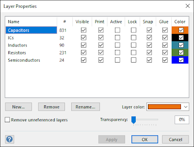
I have also created different layers for each category of components for better management and flexibility of display:


Notice that besides assigning colors to components belonging to layer, it also shows the number of objects (not components) on each layer. I say 'objects' because each component is made up of a number of basic shapes which are grouped together. And until I merged these shapes, Visio will count them as individual objects still.

At this point of my PCB-RE process, though, there's no need to do so. But having different components in their own layers enables me to turn on or off a group of components at will. And once I assign reference designators to them, it will be much easier to locate a particular component, especially since the PCB does not order them according to location placement. These are two of the advantages of using Visio to create PCB layout diagrams which are mentioned in my books.

No comments:

Post a Comment