To My Readers


If this is the first time you're visiting my blog, thank you. Whether you're interested or just curious to find out about PCB reverse engineering (PCB-RE), I hope you'll find something useful here.

This blog contains many snippets of the content in my books to provide a more detailed overall sampling for my would-be readers to be better informed before making the purchase. Of course, the book contains more photos and nice illustrations, as evidence from its cover page. Hopefully, this online trailer version will whet your appetite enough to want to get a copy for yourself.

Top Review

I started doing component level repair of electronics with (and without) schematics more than 40 years ago, which activity often involves reverse-engineering of printed circuit boards. Although over the years my technical interests have shifted into particle beam instrumentation, electron microscopy, and focused ion beam technology fields, till this day——and more often than not——PCB repairs have returned multiple multi-million-dollar accelerators, FIB, and SEM instruments back to operation, delivering great satisfaction and some profit.

Many of the methods described by Keng Tiong in great details are similar to the approaches I've developed, but some of the techniques are different, and as effective and useful as efficient and practical. Systematic approach and collection of useful information presented in his books are not only invaluable for a novice approaching PCB-level reverse engineering, but also very interesting reading and hands-on reference for professionals.

Focus on reverse engineering instead of original design provides unique perspective into workings of electronics, and in my opinion books by Keng Tiong (I've got all three of them) are must-read for anybody trying to develop good understanding of electronics——together with writings by Paul Horowitz and Winfield Hill, Phil Hobbs, Jim Williams, Bob Pease, Howard Johnson and Martin Graham, Sam Goldwasser, and other world's top electronics experts.

Valery Ray
Particle Beam Systems Technologist

Tuesday, February 28, 2017

Why Bother?

That's a reasonable question. After all, there are machines out there in the market that can do the work more quickly, accurately, and reliably in a week or less, such as those shown below:


So why even bother to learn how to do PCB reverse engineering by hand? Firstly, flying probe test systems are expensive test equipment. A basic system easily costs over $100k and that's not including the software license for the reverse engineering option. Even if your company could afford it, nobody would stick out his neck to buy one unless there is strong business justification for the purchase. And we have not yet consider the training and learning curve to familiarize its process and utilization, the yearly calibration and maintenance of the machine, and the cost of ownership just continues to add up.

What about benchtop versions with semi-automated learning of circuit traces? I can think of a number of vendors that supply such a product, namely Abi Electronics, Diagnosys, and Qmax. These products may be cheaper than a flying probe test system, but not necessary affordable, easier to use, or better in delivering quality results.

As for the simpler and lower cost pizza-box system, a basic configuration with 128 channels will set you back by about $5-7k at the time of my enquiry. Abi Electronics also sells their more powerful cabinet systems that support from 1024 to 2048 channels to reduce the amount of test clipping on the PCB, but again the cost will invariably go up too. In terms of usage, after defining the components and placement the RE software will guide the operator to clip or probe in clusters, depending on the available channels, and then learns the connectivity of the PCB. The netlist generated is then exported to another EDA tool called EdWin from Visionics, a much more user-friendly and feature-rich schematic editor.

While it sounds simple enough to clip and probe circuit clusters, my experience with Abi Electronics equipment taught me the challenge is in ensuring good electrical contact between the test clips and the component pins. This means that the PCB must be stripped clean of any conformal coating, and the test clips must also be free of oxidation and the grip must be good and not weaken as a result of mechanical fatigue from frequent use. If the PCB is surface-mounted or mixed type, you'll need an assortment of SMT test clips to do the job as well, and these QFP and PLCC test clips are by no means cheap!

So the real question is, are you prepared to fork out the money up front for a one-time or ad hoc PCB repair job that requires you to do a bit of reverse engineering? I think the answer is pretty obvious.

Saturday, February 25, 2017

What You Need to Know

While this book is intended for beginners interested to learn PCB reverse engineering, some background in electronics is preferred:

1. You should have a working knowledge, or at least be able to read schematic diagrams (that's the reason for buying this book in the first place—to re-create schematic drawings from a PCB!). It will be advantageous if you're already acquainted with the basic rules and concepts of what constitute a good schematic diagram, or better yet, if you have experience with some kind of EDA tools or software. You'll be able to skim through or skip over some of the basic information presented in later chapters.

2. You should be able to identify simple discrete devices (resistors, capacitors, diodes, transistors, MOSFETs, etc.), integrated circuit packages (DIP, SIP, PLCC, QFP, PGA, BGA, etc.) and modular components (DC/DC converter, etc.). But not to worry, I will provide useful pointers and tips along the way, when necessary.

3. You should have in your possession a good digital multimeter with the diode measurement function on top of the standard functions and know how to use it. I will also introduce other additional tools that will greatly aid you in your reverse engineering effort when we come to the appropriate chapter and topic.

4. You should be familiar with the color codes for certain discrete devices (resistors, capacitors, etc.) so you can read their values without having to constantly refer to the reference charts (I've provided quite a collection in the appendices). It's not the end of the road, however, if you're not able to remember what the color codes are; just that it will probably slow you down if there are plenty of such components on the PCB you're working on.

5. You should be acquainted with datasheets. Not that you're required to know all the component-related specifications, or understand every aspect of the device's performance. Thankfully no. But you do need to be able to find information like pin number, orientation, signal names, etc. and typical application examples provided by the manufacturer on how the device is used in real-life designs.

At first glance it may sound like quite a handful above, but trust me, it couldn't get any easier than what I have laid out as the basic skills required to get started. Before you even realize it, these would have become second nature and you'll be focusing on the real work!

Monday, February 20, 2017

Rewards for Review!

Since publishing my book in 2015, I have received a number of good reviews from international readers on Amazon in the US (.com), UK (.co.uk) and Europe (.de). To encourage more readers to give their reviews, I am offering the following bonuses as rewards:


These through-hole Visio layout symbols include DIP-300, DIP-400, DIP-600, PGAs and ZIPs with their corresponding sockets, making up more than 200 in total.


These PLCC Visio layout symbols include most of the common through-hole and SMD configuration available.


These SMD discrete Visio layout symbols include resistors, capacitors, inductors, and common diodes and transistor packages.


This Visio Power Supply layout diagram is featured on page 116 of Chapter 3 and is a very useful example for learning how to render mechanical illustration of modules.

So if you have already bought the book but have yet to write a review on Amazon, kindly do so and email me to have these bonuses delivered to you!

Friday, February 17, 2017

Freebies for My Book!

As mentioned in my book, readers who support my work through purchases are eligible to receive free resources. These include:


1. Sample Visio drawings found in the book:
    a. A3 and A4 templates (portrait and landscape)
    b. Anonymous TTF (monospace font with a slashed zero)
    c. Layout and schematic diagrams of the simple NCR SCSI adapter card (see above)
    d. Miscellaneous Visio objects


2. SMD Code Reference Book

This pdf ebook contains over 500 pages of nearly 24,000 SMT code references to help in identifying small SMD devices with markings.Useful and practical when reverse engineering SMT type PCBs, and since it is in electronic form it facilitates ease of searching without having to leaf through a thick printed hardcopy.


3. IC Master References

Most ICs contain prefixes and suffixes that are confusing and hard to decipher. I have collated a total of 152 pages of IC component prefixes and suffixes from 90 manufacturers, a ready reference on hand to refer to and know straight away what the IC component specifications are when gathering information on a PCB.


4. IC Packages and Dimensions

This ebook contains many integrated circuit packages and their dimensions which you can reference to create your own Visio layout drawings. There are a total of 109 different drawings, ranging from the standard DIP, SOJ, SOP, SSOP, TSOP to the BGA, uBGA, QFP, LQFP and PLCC, etc.


5. Visio Layering Example PCB

This PCB is featured in Chapter 5 Advanced Topics where you'll learn one of the powerful techniques to organize and display a PCB layout (applicable to schematic diagram as well, once you understand the concept).

To obtain the above freebies, email me at: ngkt@engineers.com with proof of purchase.

Thursday, February 16, 2017

Content Summary of the Book


Chapter 1

I know you're eager to get started right away, but it's good to know a little of what you're getting into before you plunge in completely. You'll need to have certain background in electronics. I'll mention some available alternatives to doing reverse engineering completely by hand, though they're not necessarily affordable unless you have deep pockets and are willing to part with your hard-earned cash. I'll also share my personal story on what started me on this journey (hopefully a good and inspiring read to you). Then there's the copyright issue which I'll give my personal take on it, before rounding up the chapter with a little work philosophy.

Chapter 2

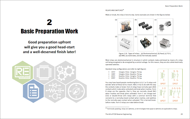
This chapter may be thought of as a practical introduction or revision to electronics in terms of the various building blocks of a PCB—resistors, capacitors, inductors, fuses, relays, diodes, zeners, transistors, MOSFETs, and ICs, etc. You may think it's boring or too elementary but I've put in quite a substantial amount of information here, so you should be able to find some rare gems among the junks (to borrow a phrase from the PCB recycle industry). I'll deal with components without markings and reference designators, touch on a bit about conformal coatings, as well as how component datasheets will be a great help later on. These elements formed what I call the ABCD's of preparation work—an essential step that will save you a lot of time and trouble when you start to do the real work.

Chapter 3

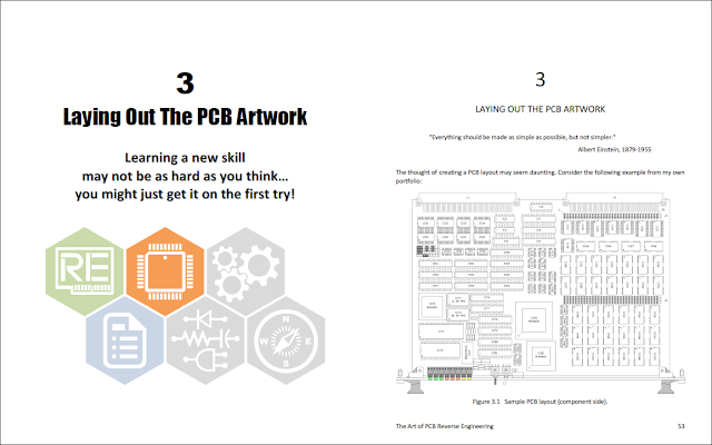
We'll get down to serious business and start doing some interesting PCB layouts and components beginning with this chapter. I will provide a brief introduction to Microsoft Visio, the diagramming software we'll be using throughout the book. You will learn how to setup and navigate the Visio workspace, familiarize yourself with its various tools and functions, decide on which template to use or begin from scratch, create your own component layouts in relation to their datasheets, and more. I have included some of my very own PCB artworks to motivate you and show you what you can possibly do with Visio.

Chapter 4

Things will get more exciting as we begin to draw the schematics of a PCB. Besides showing you how to create the various component symbols and elements of a schematic, I will also teach you the strategic approaches to reverse engineering different types of PCBs (digital, analog, power, etc.). At the same time, you will also learn why it is advantageous to have a PCB layout and BOM in the first place. Having a good sense of proportion and direction is important, especially if your schematic diagram is going to span multiple pages; I will lay down specific guidelines so you know how to plan your schematics for better readability and consistency.

Chapter 5

In this chapter, I will show you some advanced techniques you can apply to achieve a more professional level in creating both the PCB layout and schematic diagram. One word of caution: attaining mastery of anything does come with a price tag (Einstein would agree with that, being one of the greatest minds in the twentieth century). If you're willing to put in the extra efforts, I guarantee that you'll not only excel in the art of PCB reverse engineering, you'll pick up a life skill—an attitude—that will enable you to go farther, and a new found confidence to face challenges in your engineering career.

Chapter 6

There's no limit to what you can learn or do, unless you choose to stop learning or doing. I'm no motivational speaker, though I've conducted various training courses related to my work, and some outside of my work (such as MATLAB® at a friend's training company). As such, I know the importance of life-long learning and decided to devote this final chapter to discussing some possible areas of expanding your engineering knowledge and skills.

Wednesday, February 15, 2017

What This Book Is About

This book will not teach you to become proficient in using electronic design automation (EDA) tools or software to produce or re-produce PCBs from schematic entry to gerber design files. It is not even intended to give you a formal study on PCB structural design and fabrication. There are many books out there that already addressed these topics and by authors who are certainly more knowledgeable and the authority in these fields.

That said, this book does impart knowledge on PCBs that relate to the subject of reverse engineering, as a basic understanding of any PCB you intend to reverse engineer is essential to your success. Also, I will be using Microsoft® Visio albeit in a generic manner to demonstrate the steps involved. You will learn to systematically assess the PCB candidates, gather the necessary information relating to its components, create the layout diagram and parts list for reference, and use relevant strategies to find interconnections to re-create the schematic diagram, as well as other essential and useful stuff.

Free resources are made available to buyers of my book. You can email me at: ngkt@engineer.com with proof of purchase to receive them. Buyers who leave reviews on Amazon will receive additional bonuses too!

Tuesday, February 14, 2017

Some Personal Background

I was introduced to Electronics at the age of 15 in my higher secondary school days. I was one of those fortunate batches of students—in fact, the last in-take to study basic electricity and electronics in the school's curriculum in 1978.

Electronics was totally new to me, and I had problem understanding some of the basic concepts back then. It might surprise you that I had trouble figuring out the milli-, micro-, nano-, Kilo- and Mega- prefixes in Ohm's Law, struggling with corrections and re-corrections in my class assignments I almost gave up the subject for fear and frustration. Thankfully the light bulb turned on in me after a harrowing first semester, and from then on there was no looking back as I went on to do well for my final exams and did my major in Electronics and Communication for my tertiary education.

Due to family financial difficulties, I signed up with the Republic of Singapore Air Force (RSAF) after my graduation as an aircraft radar and communications (RC) technician. I did well in the Air Engineering Training Institute (AETI) and was selected for the E-2C Hawkeye program. In May of 1986, I attended a six-month training at the Grumman Aerospace Corporation's premise in Long Island, New York. There for the first time, I was introduced to the concept of automated test systems (ATS) as I learned how to operate and maintain the CAT-IIID and RADCOM test stations, and used these awesome equipment to perform test diagnostics on 75% of the E-2C's sophisticated avionics (radar, communications, navigation, displays, power supplies, etc.)

My invaluable experience as one of the pioneers in setting up the E-2C squadron's third-line repair bay and running the daily maintenance operation, as well as training three batches of local technicians, laid a solid foundation for my engineering career in electronics, so much so that I was head-hunted and invited to join Singapore Technologies (ST) Electronics Limited, a subsidiary of Singapore's home-grown defense industry, ST Engineering Limited, right after my first contract with the RSAF expired. I've been with the company since for over 23 years and now a Principal Engineer by title.

Learning is a life-long process. The same is true in electronics and in the field of test engineering, which is still my primary job scope and interest. I've worked on a variety of printed circuit boards (PCBs) from through-holes using the humble TTL logic circuits, to the high-density surface-mount type multi-layered boards containing complex VLSI, FPGA and ASIC BGA chips. The rate at which integrated circuits grow in complexity and density is staggering, especially in the last decade or so.

In this book, I will share what I've learned in my years of working on PCBs with no schematic diagrams, my approach of assessing a PCB, analyzing and reconstructing its electrical connectivity, the tools and methods I employed, useful tips to take note, as well as pitfalls to avoid. Sprinkled in the footnotes you will find some interesting anecdotes and personal takes to keep the subject of this book light-hearted and (hopefully) engaging.

Monday, February 13, 2017

Dedication

This book is dedicated to all electronics enthusiasts who share the same passion and appreciation for printed circuits and possess the curiosity and tenacity of engineers to unravel the beauty of the original design.

Acknowledgement

This book would not have been possible without the understanding and support of my wife, Bernice, when I expressed to her my desire to write a book of this nature that is totally outside her knowledge domain.

Saturday, February 11, 2017

Legal Information

All articles and illustrations found in this blog are the property of its owner. Copyright (c) 2017

Screenshots from Microsoft® Visio are used with permission from Microsoft. Both Microsoft and Visio are registered trademarks of Microsoft Corporation in and outside the United States. Products and services mentioned are trademarks or registered trademarks of their respective companies. All trademarks and registered trademarks in this site are the property of their respective holders. 

Limit of Liability and Disclaimer of Warranty

The information, examples, illustrations, documentation, and other references in this website are provided "as is", without warranty of any kind, expressed or implied, including without limitation any warranty concerning the accuracy, adequacy, or completeness of the material or the results obtained from using the material. The owner of this website shall not be held responsible for any claims attributable to errors, omissions, or other inaccuracies in the materials presented. In no event shall the owner be liable for direct, indirect, special, incidental, or consequential damages in connection with, or arising out of, the construction, performance, or other use of the materials contained herein.